 | –≠–ª–µ–∫—Ç—Ä–æ–Ω–Ω—ã–π –∫–æ–º–ø–æ–Ω–µ–Ω—Ç: 76042012A | –°–∫–∞—á–∞—Ç—å:  PDF PDF  ZIP ZIP |
SN54221, SN54LS221, SN74221, SN74LS221
DUAL MONOSTABLE MULTIVIBRATORS
WITH SCHMITT TRIGGER INPUTS
SDLS213B - DECEMBER 1983 - REVISED NOVEMBER 2004
1
POST OFFICE BOX 655303
∑
DALLAS, TEXAS 75265
D
Dual Versions of Highly Stable SN54121
and SN74121 One Shots
D
SN54221 and SN74221 Demonstrate
Electrical and Switching Characteristics
That Are Virtually Identical to the SN54121
and SN74121 One Shots
D
Pinout Is Identical to the SN54123,
SN74123, SN54LS123, and SN74LS123
D
Overriding Clear Terminates Output Pulse
TYPE
MAXIMUM
OUTPUT
PULSE
LENGTH(S)
SN54221
21
SN74221
28
SN54LS221
49
SN74LS221
70
description/ordering information
The '221 and 'LS221 devices are dual
multivibrators with performance characteristics
virtually identical to those of the '121 devices.
Each multivibrator features a negative-transition-
triggered input and a positive-transition-triggered
input, either of which can be used as an inhibit
input.
ORDERING INFORMATION
TA
PACKAGE
ORDERABLE
PART NUMBER
TOP-SIDE
MARKING
PDIP - N
Tube
SN74221N
SN74221N
PDIP - N
Tube
SN74LS221N
SN74LS221N
0
∞
C to 70
∞
C
SOIC - D
Tube
SN74LS221D
LS221
0
∞
C to 70
∞
C
SOIC - D
Tape and reel
SN74LS221DR
LS221
SOP - NS
Tape and reel
SN74LS221NSR
74LS221
SSOP - DB
Tape and reel
SN74LS221DBR
LS221
CDIP - J
Tube
SNJ54221J
SNJ54221J
-55
∞
C to 125
∞
C
CDIP - J
Tube
SNJ54LS221J
SNJ54LS221J
-55 C to 125 C
LCCC - FK
Tube
SNJ54LS221FK
SNJ54LS221FK
Package drawings, standard packing quantities, thermal data, symbolization, and PCB design guidelines are
available at www.ti.com/sc/package.
Copyright
2004, Texas Instruments Incorporated
PRODUCTION DATA information is current as of publication date.
Products conform to specifications per the terms of Texas Instruments
standard warranty. Production processing does not necessarily include
testing of all parameters.
3
2
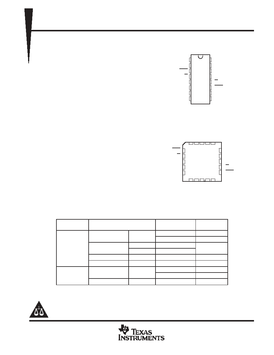
1 20 19
9 10 11 12 13
4
5
6
7
8
18
17
16
15
14
1C
ext
1Q
NC
2Q
2CLR
1CLR
1Q
NC
2Q
2C
ext
1B
1A
NC
2A
2B
V
1R
ext
GND
NC
1A
1B
1CLR
1Q
2Q
2C
ext
2R
ext
/C
ext
GND
V
CC
1R
ext
/C
ext
1C
ext
1Q
2Q
2CLR
2B
2A
SN54221, SN54LS221 . . . J PACKAGE
SN74221 . . . N PACKAGE
SN74LS221 . . . D, DB, N, OR NS PACKAGE
(TOP VIEW)
SN54LS221 . . . FK PACKAGE
(TOP VIEW)
1
2
3
4
5
6
7
8
16
15
14
13
12
11
10
9
CC
ext
/C
ext
2R
/C
ext
NC - No internal connection
On products compliant to MIL PRF 38535, all parameters are tested
unless otherwise noted. On all other products, production
processing does not necessarily include testing of all parameters.
Please be aware that an important notice concerning availability, standard warranty, and use in critical applications of
Texas Instruments semiconductor products and disclaimers thereto appears at the end of this data sheet.

SN54221, SN54LS221, SN74221, SN74LS221
DUAL MONOSTABLE MULTIVIBRATORS
WITH SCHMITT TRIGGER INPUTS
SDLS213B - DECEMBER 1983 - REVISED NOVEMBER 2004
2
POST OFFICE BOX 655303
∑
DALLAS, TEXAS 75265
description/ordering information (continued)
Pulse triggering occurs at a particular voltage level and is not directly related to the transition time of the input
pulse. Schmitt-trigger input circuitry (TTL hysteresis) for B input allows jitter-free triggering from inputs with
transition at rates as slow as 1 V/s, providing the circuit with excellent noise immunity, typically of 1.2 V. A high
immunity to V
CC
noise, typically of 1.5 V, also is provided by internal latching circuitry.
Once fired, the outputs are independent of further transitions of the A and B inputs and are a function of the timing
components, or the output pulses can be terminated by the overriding clear. Input pulses can be of any duration
relative to the output pulse. Output pulse length can be varied from 35 ns to the maximum by choosing
appropriate timing components. With R
ext
= 2 k
and C
ext
= 0, an output pulse typically of 30 ns is achieved
that can be used as a dc-triggered reset signal. Output rise and fall times are TTL compatible and independent
of pulse length. Typical triggering and clearing sequences are shown as a part of the switching characteristics
waveforms.
Pulse-width stability is achieved through internal compensation and is virtually independent of V
CC
and
temperature. In most applications, pulse stability is limited only by the accuracy of external timing components.
Jitter-free operation is maintained over the full temperature and V
CC
ranges for more than six decades of timing
capacitance (10 pF to 10
µ
F) and more than one decade of timing resistance (2 k
to 30 k
for the SN54221,
2 k
to 40 k
for the SN74221, 2 k
to 70 k
for the SN54LS221, and 2 k
to 100 k
for the SN74LS221).
Throughout these ranges, pulse width is defined by the relationship: t
w
(out) = C
ext
R
ext
In2
0.7 C
ext
R
ext
. In
circuits where pulse cutoff is not critical, timing capacitance up to 1000
µ
F and timing resistance as low as 1.4 k
can be used. Also, the range of jitter-free output pulse widths is extended if V
CC
is held to 5 V and free-air
temperature is 25
∞
C. Duty cycles as high as 90% are achieved when using maximum recommended R
T
. Higher
duty cycles are available if a certain amount of pulse-width jitter is allowed.
The variance in output pulse width from device to device typically is less than
±
0.5% for given external timing
components. An example of this distribution for the '221 is shown in Figure 3. Variations in output pulse width
versus supply voltage and temperature for the '221 are shown in Figures 4 and 5, respectively.
Pin assignments for these devices are identical to those of the SN54123/SN74123 or SN54LS123/SN74LS123
so that the '221 or 'LS221 devices can be substituted for those products in systems not using the retrigger by
merely changing the value of R
ext
and/or C
ext
; however, the polarity of the capacitor must be changed.
FUNCTION TABLE
(each monostable multivibrator)
INPUTS
OUTPUTS
CLR
A
B
Q
Q
L
X
X
L
H
X
H
X
L
H
X
X
L
L
H
H
L
H
H
L
H
Pulsed-output patterns are tested during
AC switching at 25
∞
C with Rext = 2 k
, and
Cext = 80 pF.
This condition is true only if the output of
the latch formed by the two NAND gates
has been conditioned to the logic 1 state
prior to CLR going high. This latch is
conditioned by taking either A high or
B low while CLR is inactive (high).

SN54221, SN54LS221, SN74221, SN74LS221
DUAL MONOSTABLE MULTIVIBRATORS
WITH SCHMITT TRIGGER INPUTS
SDLS213B - DECEMBER 1983 - REVISED NOVEMBER 2004
3
POST OFFICE BOX 655303
∑
DALLAS, TEXAS 75265
timing component connections
VCC
Rext
To Cext
Terminal
To Rext/Cext
Terminal
NOTE: Due to the internal circuit, the Rext/Cext terminal never is more positive than the Cext terminal.

SN54221, SN54LS221, SN74221, SN74LS221
DUAL MONOSTABLE MULTIVIBRATORS
WITH SCHMITT TRIGGER INPUTS
SDLS213B - DECEMBER 1983 - REVISED NOVEMBER 2004
4
POST OFFICE BOX 655303
∑
DALLAS, TEXAS 75265
schematics of inputs and outputs
VCC
Req
Input
VCC
100
NOM
Output
EQUIVALENT OF EACH INPUT
TYPICAL OF ALL OUTPUTS
SN54/74221
SN54/74LS221
EQUIVALENT OF EACH INPUT
TYPICAL OF ALL OUTPUTS
VCC
Req
Input
VCC
Output
120
NOM
A Input: Req = 4 k
NOM
B, CLR Input: Req = 2 k
NOM
A Input: Req = 25 k
NOM
B Input: Req = 15.4 k
NOM
CLR: Req = 12.5 k
NOM

SN54221, SN54LS221, SN74221, SN74LS221
DUAL MONOSTABLE MULTIVIBRATORS
WITH SCHMITT TRIGGER INPUTS
SDLS213B - DECEMBER 1983 - REVISED NOVEMBER 2004
5
POST OFFICE BOX 655303
∑
DALLAS, TEXAS 75265
absolute maximum ratings over operating free-air temperature range (unless otherwise noted)
Supply voltage range, V
CC
7 V
. . . . . . . . . . . . . . . . . . . . . . . . . . . . . . . . . . . . . . . . . . . . . . . . . . . . . . . . . . . . . . . . . . .
Input voltage range, V
I
(see Note 1): 'LS221
7 V
. . . . . . . . . . . . . . . . . . . . . . . . . . . . . . . . . . . . . . . . . . . . . . . . . . .
'221 5.5
V
. . . . . . . . . . . . . . . . . . . . . . . . . . . . . . . . . . . . . . . . . . . . . . . . . . . .
Package thermal impedance,
JA
(see Note 2): D package
73
∞
C/W
. . . . . . . . . . . . . . . . . . . . . . . . . . . . . . . . . . .
DB package
82
∞
C/W
. . . . . . . . . . . . . . . . . . . . . . . . . . . . . . . . .
N package
67
∞
C/W
. . . . . . . . . . . . . . . . . . . . . . . . . . . . . . . . . . .
NS package
64
∞
C/W
. . . . . . . . . . . . . . . . . . . . . . . . . . . . . . . . .
Storage temperature range, T
stg
-65
∞
C to 150
∞
C
. . . . . . . . . . . . . . . . . . . . . . . . . . . . . . . . . . . . . . . . . . . . . . . . . . .
Stresses beyond those listed under "absolute maximum ratings" may cause permanent damage to the device. These are stress ratings only, and
functional operation of the device at these or any other conditions beyond those indicated under "recommended operating conditions" is not
implied. Exposure to absolute-maximum-rated conditions for extended periods may affect device reliability.
NOTES:
1. The input and output negative-voltage ratings may be exceeded if the input and output clamp-current ratings are observed.
2. The package thermal impedance is calculated in accordance with JESD 51-7.
recommended operating conditions (see Note 3)
SN54221
SN74221
UNIT
MIN
NOM
MAX
MIN
NOM
MAX
UNIT
VCC
Supply voltage
4.5
5
5.5
4.75
5
5.25
V
IOH
High-level output current
-800
-800
µ
A
IOL
Low-level output current
16
16
mA
v/
t
Rise or fall of input pulse rate
B input
1*
1
V/s
v/
t
Rise or fall of input pulse rate
A input
1*
1
V/
µ
s
TA
Operating free-air temperature
-55
125
0
70
∞
C
On products compliant to MIL-PRF-38535, this parameter is not production tested.
NOTE 3: All unused inputs of the device must be held at VCC or GND to ensure proper device operation. Refer to the TI application report,
Implications of Slow or Floating CMOS Inputs, literature number SCBA004.

SN54221, SN54LS221, SN74221, SN74LS221
DUAL MONOSTABLE MULTIVIBRATORS
WITH SCHMITT TRIGGER INPUTS
SDLS213B - DECEMBER 1983 - REVISED NOVEMBER 2004
6
POST OFFICE BOX 655303
∑
DALLAS, TEXAS 75265
electrical characteristics over recommended operating free-air temperature range (unless
otherwise noted)
PARAMETER
TEST CONDITIONS
SN54221
SN74221
UNIT
PARAMETER
TEST CONDITIONS
MIN
TYP
MAX
MIN
TYP
MAX
UNIT
VT+
Positive-going threshold voltage,
B input
VCC = MIN
1.55
2*
1.55
2
V
VT-
Negative-going threshold voltage,
B input
VCC = MIN
0.8*
1.35
0.8
1.35
V
VIK
VCC = MIN,
II = -12 mA
-1.5
-1.5
V
VOH
VCC = MIN,
IOH = -800
µ
A
2.4
3.4
2.4
3.4
V
VOL
VCC = MIN,
IOL = 16 mA
0.2
0.4
0.2
0.4
V
II
VCC = MAX,
VI = 5.5 V
1
1
mA
IIH
A input
VCC = MAX,
VI = 2.4 V
40
40
A
IIH
CLR, B input
VCC = MAX,
VI = 2.4 V
80
80
µ
A
IIL
A input
VCC = MAX,
VI = 0.4 V
-1.6
-1.6
mA
IIL
CLR, B input
VCC = MAX,
VI = 0.4 V
-3.2
-3.2
mA
IOSß
VCC = MAX
-20
-55
-18
-55
mA
ICC
Quiescent
VCC = MAX
26
50*
26
50
mA
ICC
Triggered
VCC = MAX
46
80*
46
80
mA
On products compliant to MIL-PRF-38535, this parameter is not production tested.
For conditions shown as MIN or MAX, use the appropriate value specified under recommended operating conditions.
All typical values are at VCC = 5 V, TA = 25
∞
C.
ß Not more than one output should be shorted at a time, and the duration of the short circuit should not exceed one second.
timing requirements over recommended ranges of supply voltage and operating free-air
temperature
SN54221
SN74221
UNIT
MIN
MAX
MIN
MAX
UNIT
tw
Pulse duration
A or B input
50
50
ns
tw
Pulse duration
CLR
20
20
ns
tsu
Setup time, inactive-state∂
CLR
15
15
ns
Rext
External timing resistance
1.4*
30*
1.4
40
k
Cext
External timing capacitance
0*
1000*
0
1000
µ
F
Output duty cycle
Rext = 2 k
67%
67%
Output duty cycle
Rext = MAX Rext
90%
90%
On products compliant to MIL-PRF-38535, this parameter is not production tested.
∂ Inactive-state setup time also is referred to as recovery time.

SN54221, SN54LS221, SN74221, SN74LS221
DUAL MONOSTABLE MULTIVIBRATORS
WITH SCHMITT TRIGGER INPUTS
SDLS213B - DECEMBER 1983 - REVISED NOVEMBER 2004
7
POST OFFICE BOX 655303
∑
DALLAS, TEXAS 75265
switching characteristics V
CC
= 5 V, R
L
= 400
,
T
A
= 25
_
C (see Figures 1 and 2)
PARAMETER
FROM
TO
TEST CONDITIONS
SN54221
SN74221
UNIT
PARAMETER
FROM
(INPUT)
TO
(OUTPUT)
TEST CONDITIONS
MIN
TYP
MAX
MIN
TYP
MAX
UNIT
tPLH
A
Q
45
70
45
70
tPLH
B
Q
Cext = 80 pF,
Rext = 2 k
35
55
35
55
ns
tPHL
A
Q
Cext = 80 pF,
Rext = 2 k
50
80
50
80
ns
tPHL
B
Q
40
65
40
65
tPHL
CLR
Q
Cext = 80 pF,
Rext = 2 k
27
27
ns
tPLH
CLR
Q
Cext = 80 pF,
Rext = 2 k
40
40
ns
Cext = 80 pF,
Rext = 2 k
70
110
150
70
110
150
tw
A or B
Q or Q
Cext = 0,
Rext = 2 k
17
30
50
17
30
50
ns
tw
A or B
Q or Q
Cext = 100 pF, Rext = 10 k
650
700
750
650
700
750
ns
Cext = 1
µ
F,
Rext = 10 k
6.5*
7
7.5*
6.5
7
7.5
ms
On products compliant to MIL-PRF-38535, this parameter is not production tested.
recommended operating conditions (see Note 4)
SN54LS221
SN74LS221
UNIT
MIN
NOM
MAX
MIN
NOM
MAX
UNIT
VCC
Supply voltage
4.5
5
5.5
4.75
5
5.25
V
IOH
High-level output current
-400
-400
µ
A
IOL
Low-level output current
4
8
mA
v/
t
Rise or fall of input pulse rate
B input
1*
1
V/s
v/
t
Rise or fall of input pulse rate
A input
1*
1
V/
µ
s
TA
Operating free-air temperature
-55
125
0
70
∞
C
On products compliant to MIL-PRF-38535, this parameter is not production tested.
NOTE 4: All unused inputs of the device must be held at VCC or GND to ensure proper device operation. Refer to the TI application report,
Implications of Slow or Floating CMOS Inputs, literature number SCBA004.
SN54221, SN54LS221, SN74221, SN74LS221
DUAL MONOSTABLE MULTIVIBRATORS
WITH SCHMITT TRIGGER INPUTS
SDLS213B - DECEMBER 1983 - REVISED NOVEMBER 2004
8
POST OFFICE BOX 655303
∑
DALLAS, TEXAS 75265
electrical characteristics over recommended operating free-air temperature range (unless
otherwise noted)
PARAMETER
TEST CONDITIONS
SN54LS221
SN74LS221
UNIT
PARAMETER
TEST CONDITIONS
MIN
TYP
MAX
MIN
TYP
MAX
UNIT
VT+
Positive-going threshold voltage,
B input
VCC = MIN
1
2*
1
2
V
VT-
Negative-going threshold voltage,
B input
VCC = MIN
0.7*
0.9
0.8
0.9
V
VIK
VCC = MIN,
II = -18 mA
-1.5
-1.5
V
VOH
VCC = MIN,
IOH = -400
µ
A
2.5
3.4
2.7
3.4
V
VOL
VCC = MIN
IOL = 4 mA
0.25
0.4
0.25
0.4
V
VOL
VCC = MIN
IOL = 8 mA
0.35
0.5
V
II
VCC = MAX,
VI = 7 V
0.1
0.1
mA
IIH
VCC = MAX,
VI = 2.7 V
20
20
µ
A
IIL
A input
VCC = MAX,
VI = 0.4 V
-0.4
-0.4
mA
IIL
CLR, B input
VCC = MAX,
VI = 0.4 V
-0.8
-0.8
mA
IOSß
VCC = MAX
-20
-100
-20
-100
mA
ICC
Quiescent
VCC = MAX
4.7
11
4.7
11
mA
ICC
Triggered
VCC = MAX
19
27*
19
27
mA
On products compliant to MIL-PRF-38535, this parameter is not production tested.
For conditions shown as MIN or MAX, use the appropriate value specified under recommended operating conditions.
All typical values are at VCC = 5 V, TA = 25
∞
C.
ß Not more than one output should be shorted at a time, and the duration of the short circuit should not exceed one second.
timing requirements over recommended ranges of supply voltage and operating free-air
temperature
SN54LS221
SN74LS221
UNIT
MIN
MAX
MIN
MAX
UNIT
tw
Pulse duration
A or B
50
50
ns
tw
Pulse duration
CLR
40
40
ns
tsu
Setup time, inactive state∂
CLR
15
15
ns
Rext
External timing resistance
1.4*
70*
1.4
100
k
Cext
External timing capacitance
0*
1000*
0
1000
µ
F
Output duty cycle
RT = 2 k
50%
50%
Output duty cycle
RT = MAX Rext
90%
90%
On products compliant to MIL-PRF-38535, this parameter is not production tested.
∂ Inactive-state setup time also is referred to as recovery time.
SN54221, SN54LS221, SN74221, SN74LS221
DUAL MONOSTABLE MULTIVIBRATORS
WITH SCHMITT TRIGGER INPUTS
SDLS213B - DECEMBER 1983 - REVISED NOVEMBER 2004
9
POST OFFICE BOX 655303
∑
DALLAS, TEXAS 75265
switching characteristics V
CC
= 5 V, R
L
= 2 k
,
T
A
= 25
_
C (see Figures 1 and 2)
PARAMETER
FROM
TO
TEST CONDITIONS
SN54LS221
SN74LS221
UNIT
PARAMETER
FROM
(INPUT)
TO
(OUTPUT)
TEST CONDITIONS
MIN
TYP
MAX
MIN
TYP
MAX
UNIT
tPLH
A
Q
45
70
45
70
tPLH
B
Q
Cext = 80 pF,
Rext = 2 k
35
55
35
55
ns
tPHL
A
Q
Cext = 80 pF,
Rext = 2 k
50
80
50
80
ns
tPHL
B
Q
40
65
40
65
tPHL
CLR
Q
Cext = 80 pF,
Rext = 2 k
35
55
35
55
ns
tPLH
CLR
Q
Cext = 80 pF,
Rext = 2 k
44
65
44
65
ns
Cext = 80 pF,
Rext = 2 k
70
120
150
70
120
150
tw
A or B
Q or Q
Cext = 0,
Rext = 2 k
20
47
70
20
47
70
ns
tw
A or B
Q or Q
Cext = 100 pF, Rext = 10 k
670
740
810
670
740
810
ns
Cext = 1
µ
F,
Rext = 10 k
6*
6.9
7.5*
6
6.9
7.5
ms
On products compliant to MIL-PRF-38535, this parameter is not production tested.

SN54221, SN54LS221, SN74221, SN74LS221
DUAL MONOSTABLE MULTIVIBRATORS
WITH SCHMITT TRIGGER INPUTS
SDLS213B - DECEMBER 1983 - REVISED NOVEMBER 2004
10
POST OFFICE BOX 655303
∑
DALLAS, TEXAS 75265
PARAMETER MEASUREMENT INFORMATION
B
CLR
Q
Q
3 V
3 V
0 V
0 V
VOH
VOH
VOL
VOL
tw
60 ns
tPLH
tPHL
tPHL
tPLH
CONDITION 1: TRIGGER FROM B, THEN CLR
B
CLR
Q
3 V
3 V
0 V
0 V
VOH
VOL
60 ns
CONDITION 2: TRIGGER FROM B, THEN CLR
B
CLR
Q
3 V
3 V
0 V
0 V
VOH
VOL
50 ns
CONDITION 3: CLR OVERRIDING B, THEN TRIGGER FROM B
tsu
0
tw
Triggered
Not Triggered
A is low.
Figure 1. Switching Characteristics

SN54221, SN54LS221, SN74221, SN74LS221
DUAL MONOSTABLE MULTIVIBRATORS
WITH SCHMITT TRIGGER INPUTS
SDLS213B - DECEMBER 1983 - REVISED NOVEMBER 2004
11
POST OFFICE BOX 655303
∑
DALLAS, TEXAS 75265
PARAMETER MEASUREMENT INFORMATION
B
CLR
Q
3 V
3 V
0 V
0 V
VOH
VOL
50 ns
CONDITION 4: TRIGGERING FROM POSITIVE TRANSITION OF CLR
50 ns
A
CLR
Q
Q
3 V
3 V
0 V
0 V
VOH
VOH
VOL
VOL
tw
60 ns
tPLH
tPHL
tPHL
tPLH
CONDITION 5: TRIGGER FROM A, THEN CLR
A
Q
Q
3 V
0 V
VOH
VOH
VOL
VOL
tw
CONDITION 6: TRIGGER FROM A
tw
A is low.
B and CLR are high.
NOTES: A. Input pulses are supplied by generators having the following characteristics: PRR
1 MHz, ZO
50
; for SN54/74221, tr
7 ns,
tf
7 ns, for SN54/74LS221, tr
15 ns, tf
6 ns.
B. All measurements are made between the 1.5-V points of the indicated transitions for the SN54/74221 or between the 1.3-V points
for the SN54/74LS221.
Figure 1. Switching Characteristics (Continued)

SN54221, SN54LS221, SN74221, SN74LS221
DUAL MONOSTABLE MULTIVIBRATORS
WITH SCHMITT TRIGGER INPUTS
SDLS213B - DECEMBER 1983 - REVISED NOVEMBER 2004
12
POST OFFICE BOX 655303
∑
DALLAS, TEXAS 75265
PARAMETER MEASUREMENT INFORMATION
tPHL
tPLH
tPLH
tPHL
3 V
3 V
0 V
0 V
th
tsu
VOLTAGE WAVEFORMS
SETUP AND HOLD TIMES
Timing
Input
Data
Input
High-Level
Pulse
Low-Level
Pulse
tw
VOLTAGE WAVEFORMS
PULSE DURATIONS
Input
Out-of-Phase
Output
3 V
0 V
VOL
VOH
VOH
VOL
In-Phase
Output
VOLTAGE WAVEFORMS
PROPAGATION DELAY TIMES
LOAD CIRCUIT FOR
BI-STATE
TOTEM-POLE OUTPUTS
(see Note B)
VCC
RL
From Output
Under Test
CL = 15 pF
(see Note A)
Test
Point
NOTES: A. CL includes probe and jig capacitance.
B. All diodes are 1N3064 or equivalent.
C. In the examples above, the phase relationships between inputs and outputs have been chosen arbitrarily.
D. All input pulses are supplied by generators having the following characteristics: PRR
1 MHz, ZO
50
and, for SN54/74221,
tr
7 ns, tf
7 ns, for SN54/74LS221, tr
15 ns, tf
6 ns.
E. All measurements are made between the 1.5-V points of the indicated transitions for the SN54/74221 or between the 1.3-V points
for the SN54/74LS221.
Figure 2. Load Circuits and Voltage Waveforms

SN54221, SN54LS221, SN74221, SN74LS221
DUAL MONOSTABLE MULTIVIBRATORS
WITH SCHMITT TRIGGER INPUTS
SDLS213B - DECEMBER 1983 - REVISED NOVEMBER 2004
13
POST OFFICE BOX 655303
∑
DALLAS, TEXAS 75265
TYPICAL CHARACTERISTICS (SN54/74221 ONLY)
Figure 3
Median
Relative Frequency of Occurrence
DISTRIBUTION OF UNITS
FOR
OUTPUT PULSE
tw - Output Pulse
VCC = 5 V
TA = 25
∞
C
Median
+0.5%
Median
+0.5%
Figure 4
0
- 0.5
-1
4.5
4.75
5
0.5
VARIATION IN OUTPUT PULSE
vs
SUPPLY VOLTAGE
1
5.25
5.5
-
V
ariation in Output Pulse - %
t
w
VCC - Supply Voltage - V
Cext = 60 pF
Rext = 10 k
TA = 25
∞
C
tw
420 ns
at VCC = 5 V
Figure 5
-25
-50
-75
0
- 0.5
-1
0
25
50
-
V
ariation in Output Pulse - %
0.5
VARIATION IN OUTPUT PULSE
vs
FREE-AIR TEMPERATURE
1
75
100
125
TA - Free-Air Temperature -
∞
C
t
w
VCC = 5 V
Cext = 60 pF
Rext = 10 k
tw
420 ns
at TA = 25
∞
C
OUTPUT PULSE
vs
TIMING RESISTOR VALUE
Figure 6
100 ns
10 ns
1
2
4
7 10
10 ms
1 ms
20
40
70 100
- Output Pulse
t
w
100
µ
s
10
µ
s
1
µ
s
VCC = 5 V
TA = 25
∞
C
F
µ
Cext = 1
F
µ
Cext = 0.1
F
µ
Cext = 0.01
Cext = 1000 pF
Cext = 100 pF
Cext = 10 pF
See Note A
Rext - Timing Resistor Value - k
Data for temperatures below 0
∞
C and above 70
∞
C, and for supply voltages below 4.75 V and above 5.25 V are applicable for the SN54221 only.
NOTE A: These values of resistance exceed the maximum recommended for use over the full military temperature range of the SN54221.
PACKAGING INFORMATION
Orderable Device
Status
(1)
Package
Type
Package
Drawing
Pins Package
Qty
Eco Plan
(2)
Lead/Ball Finish
MSL Peak Temp
(3)
5962-8771101EA
ACTIVE
CDIP
J
16
1
TBD
Call TI
Level-NC-NC-NC
76042012A
ACTIVE
LCCC
FK
20
1
TBD
Call TI
Level-NC-NC-NC
7604201EA
ACTIVE
CDIP
J
16
1
TBD
Call TI
Level-NC-NC-NC
7604201FA
ACTIVE
CFP
W
16
1
TBD
Call TI
Level-NC-NC-NC
JM38510/31402B2A
ACTIVE
LCCC
FK
20
1
TBD
Call TI
Level-NC-NC-NC
JM38510/31402BEA
ACTIVE
CDIP
J
16
1
TBD
Call TI
Level-NC-NC-NC
JM38510/31402BFA
ACTIVE
CFP
W
16
1
TBD
Call TI
Level-NC-NC-NC
SN54221J
ACTIVE
CDIP
J
16
1
TBD
Call TI
Level-NC-NC-NC
SN54LS221J
ACTIVE
CDIP
J
16
1
TBD
Call TI
Level-NC-NC-NC
SN74221N
ACTIVE
PDIP
N
16
25
Pb-Free
(RoHS)
CU NIPDAU
Level-NC-NC-NC
SN74221NE4
ACTIVE
PDIP
N
16
25
Pb-Free
(RoHS)
CU NIPDAU
Level-NC-NC-NC
SN74LS221D
ACTIVE
SOIC
D
16
40
Green (RoHS &
no Sb/Br)
CU NIPDAU
Level-1-260C-UNLIM
SN74LS221DBR
ACTIVE
SSOP
DB
16
2000 Green (RoHS &
no Sb/Br)
CU NIPDAU
Level-1-260C-UNLIM
SN74LS221DBRE4
ACTIVE
SSOP
DB
16
2000 Green (RoHS &
no Sb/Br)
CU NIPDAU
Level-1-260C-UNLIM
SN74LS221DE4
ACTIVE
SOIC
D
16
40
Green (RoHS &
no Sb/Br)
CU NIPDAU
Level-1-260C-UNLIM
SN74LS221DR
ACTIVE
SOIC
D
16
2500 Green (RoHS &
no Sb/Br)
CU NIPDAU
Level-1-260C-UNLIM
SN74LS221DRE4
ACTIVE
SOIC
D
16
2500 Green (RoHS &
no Sb/Br)
CU NIPDAU
Level-1-260C-UNLIM
SN74LS221N
ACTIVE
PDIP
N
16
25
Pb-Free
(RoHS)
CU NIPDAU
Level-NC-NC-NC
SN74LS221N3
OBSOLETE
PDIP
N
16
TBD
Call TI
Call TI
SN74LS221NE4
ACTIVE
PDIP
N
16
25
Pb-Free
(RoHS)
CU NIPDAU
Level-NC-NC-NC
SN74LS221NSR
ACTIVE
SO
NS
16
2000 Green (RoHS &
no Sb/Br)
CU NIPDAU
Level-1-260C-UNLIM
SN74LS221NSRE4
ACTIVE
SO
NS
16
2000 Green (RoHS &
no Sb/Br)
CU NIPDAU
Level-1-260C-UNLIM
SNJ54221J
ACTIVE
CDIP
J
16
1
TBD
Call TI
Level-NC-NC-NC
SNJ54LS221FK
ACTIVE
LCCC
FK
20
1
TBD
Call TI
Level-NC-NC-NC
SNJ54LS221J
ACTIVE
CDIP
J
16
1
TBD
Call TI
Level-NC-NC-NC
SNJ54LS221W
ACTIVE
CFP
W
16
1
TBD
Call TI
Level-NC-NC-NC
(1)
The marketing status values are defined as follows:
ACTIVE: Product device recommended for new designs.
LIFEBUY: TI has announced that the device will be discontinued, and a lifetime-buy period is in effect.
NRND: Not recommended for new designs. Device is in production to support existing customers, but TI does not recommend using this part in
a new design.
PREVIEW: Device has been announced but is not in production. Samples may or may not be available.
OBSOLETE: TI has discontinued the production of the device.
(2)
Eco
Plan
-
The
planned
eco-friendly
classification:
Pb-Free
(RoHS)
or
Green
(RoHS
&
no
Sb/Br)
-
please
check
PACKAGE OPTION ADDENDUM
www.ti.com
26-Sep-2005
Addendum-Page 1

http://www.ti.com/productcontent
for the latest availability information and additional product content details.
TBD: The Pb-Free/Green conversion plan has not been defined.
Pb-Free (RoHS): TI's terms "Lead-Free" or "Pb-Free" mean semiconductor products that are compatible with the current RoHS requirements
for all 6 substances, including the requirement that lead not exceed 0.1% by weight in homogeneous materials. Where designed to be soldered
at high temperatures, TI Pb-Free products are suitable for use in specified lead-free processes.
Green (RoHS & no Sb/Br): TI defines "Green" to mean Pb-Free (RoHS compatible), and free of Bromine (Br) and Antimony (Sb) based flame
retardants (Br or Sb do not exceed 0.1% by weight in homogeneous material)
(3)
MSL, Peak Temp. -- The Moisture Sensitivity Level rating according to the JEDEC industry standard classifications, and peak solder
temperature.
Important Information and Disclaimer:The information provided on this page represents TI's knowledge and belief as of the date that it is
provided. TI bases its knowledge and belief on information provided by third parties, and makes no representation or warranty as to the
accuracy of such information. Efforts are underway to better integrate information from third parties. TI has taken and continues to take
reasonable steps to provide representative and accurate information but may not have conducted destructive testing or chemical analysis on
incoming materials and chemicals. TI and TI suppliers consider certain information to be proprietary, and thus CAS numbers and other limited
information may not be available for release.
In no event shall TI's liability arising out of such information exceed the total purchase price of the TI part(s) at issue in this document sold by TI
to Customer on an annual basis.
PACKAGE OPTION ADDENDUM
www.ti.com
26-Sep-2005
Addendum-Page 2


MECHANICAL DATA
MLCC006B ≠ OCTOBER 1996
POST OFFICE BOX 655303
∑
DALLAS, TEXAS 75265
FK (S-CQCC-N**)
LEADLESS CERAMIC CHIP CARRIER
4040140 / D 10/96
28 TERMINAL SHOWN
B
0.358
(9,09)
MAX
(11,63)
0.560
(14,22)
0.560
0.458
0.858
(21,8)
1.063
(27,0)
(14,22)
A
NO. OF
MIN
MAX
0.358
0.660
0.761
0.458
0.342
(8,69)
MIN
(11,23)
(16,26)
0.640
0.739
0.442
(9,09)
(11,63)
(16,76)
0.962
1.165
(23,83)
0.938
(28,99)
1.141
(24,43)
(29,59)
(19,32)
(18,78)
**
20
28
52
44
68
84
0.020 (0,51)
TERMINALS
0.080 (2,03)
0.064 (1,63)
(7,80)
0.307
(10,31)
0.406
(12,58)
0.495
(12,58)
0.495
(21,6)
0.850
(26,6)
1.047
0.045 (1,14)
0.045 (1,14)
0.035 (0,89)
0.035 (0,89)
0.010 (0,25)
12
13
14
15
16
18
17
11
10
8
9
7
5
4
3
2
0.020 (0,51)
0.010 (0,25)
6
1
28
26
27
19
21
B SQ
A SQ
22
23
24
25
20
0.055 (1,40)
0.045 (1,14)
0.028 (0,71)
0.022 (0,54)
0.050 (1,27)
NOTES: A. All linear dimensions are in inches (millimeters).
B. This drawing is subject to change without notice.
C. This package can be hermetically sealed with a metal lid.
D. The terminals are gold plated.
E. Falls within JEDEC MS-004

MECHANICAL DATA
MSSO002E ≠ JANUARY 1995 ≠ REVISED DECEMBER 2001
POST OFFICE BOX 655303
∑
DALLAS, TEXAS 75265
DB (R-PDSO-G**)
PLASTIC SMALL-OUTLINE
4040065 /E 12/01
28 PINS SHOWN
Gage Plane
8,20
7,40
0,55
0,95
0,25
38
12,90
12,30
28
10,50
24
8,50
Seating Plane
9,90
7,90
30
10,50
9,90
0,38
5,60
5,00
15
0,22
14
A
28
1
20
16
6,50
6,50
14
0,05 MIN
5,90
5,90
DIM
A MAX
A MIN
PINS **
2,00 MAX
6,90
7,50
0,65
M
0,15
0
∞
≠ 8
∞
0,10
0,09
0,25
NOTES: A. All linear dimensions are in millimeters.
B. This drawing is subject to change without notice.
C. Body dimensions do not include mold flash or protrusion not to exceed 0,15.
D. Falls within JEDEC MO-150

IMPORTANT NOTICE
Texas Instruments Incorporated and its subsidiaries (TI) reserve the right to make corrections, modifications,
enhancements, improvements, and other changes to its products and services at any time and to discontinue
any product or service without notice. Customers should obtain the latest relevant information before placing
orders and should verify that such information is current and complete. All products are sold subject to TI's terms
and conditions of sale supplied at the time of order acknowledgment.
TI warrants performance of its hardware products to the specifications applicable at the time of sale in
accordance with TI's standard warranty. Testing and other quality control techniques are used to the extent TI
deems necessary to support this warranty. Except where mandated by government requirements, testing of all
parameters of each product is not necessarily performed.
TI assumes no liability for applications assistance or customer product design. Customers are responsible for
their products and applications using TI components. To minimize the risks associated with customer products
and applications, customers should provide adequate design and operating safeguards.
TI does not warrant or represent that any license, either express or implied, is granted under any TI patent right,
copyright, mask work right, or other TI intellectual property right relating to any combination, machine, or process
in which TI products or services are used. Information published by TI regarding third-party products or services
does not constitute a license from TI to use such products or services or a warranty or endorsement thereof.
Use of such information may require a license from a third party under the patents or other intellectual property
of the third party, or a license from TI under the patents or other intellectual property of TI.
Reproduction of information in TI data books or data sheets is permissible only if reproduction is without
alteration and is accompanied by all associated warranties, conditions, limitations, and notices. Reproduction
of this information with alteration is an unfair and deceptive business practice. TI is not responsible or liable for
such altered documentation.
Resale of TI products or services with statements different from or beyond the parameters stated by TI for that
product or service voids all express and any implied warranties for the associated TI product or service and
is an unfair and deceptive business practice. TI is not responsible or liable for any such statements.
Following are URLs where you can obtain information on other Texas Instruments products and application
solutions:
Products
Applications
Amplifiers
amplifier.ti.com
Audio
www.ti.com/audio
Data Converters
dataconverter.ti.com
Automotive
www.ti.com/automotive
DSP
dsp.ti.com
Broadband
www.ti.com/broadband
Interface
interface.ti.com
Digital Control
www.ti.com/digitalcontrol
Logic
logic.ti.com
Military
www.ti.com/military
Power Mgmt
power.ti.com
Optical Networking
www.ti.com/opticalnetwork
Microcontrollers
microcontroller.ti.com
Security
www.ti.com/security
Telephony
www.ti.com/telephony
Video & Imaging
www.ti.com/video
Wireless
www.ti.com/wireless
Mailing Address:
Texas Instruments
Post Office Box 655303 Dallas, Texas 75265
Copyright
2005, Texas Instruments Incorporated